- 您现在的位置:买卖IC网 > Sheet目录337 > LT3498EDDB#TRPBF (Linear Technology)IC LED DRVR WT/OLED BCKLGT 12DFN
LT3498
TYPICAL PERFORMANCE CHARACTERISTICS
T A = 25°C, unless otherwise speci?ed.
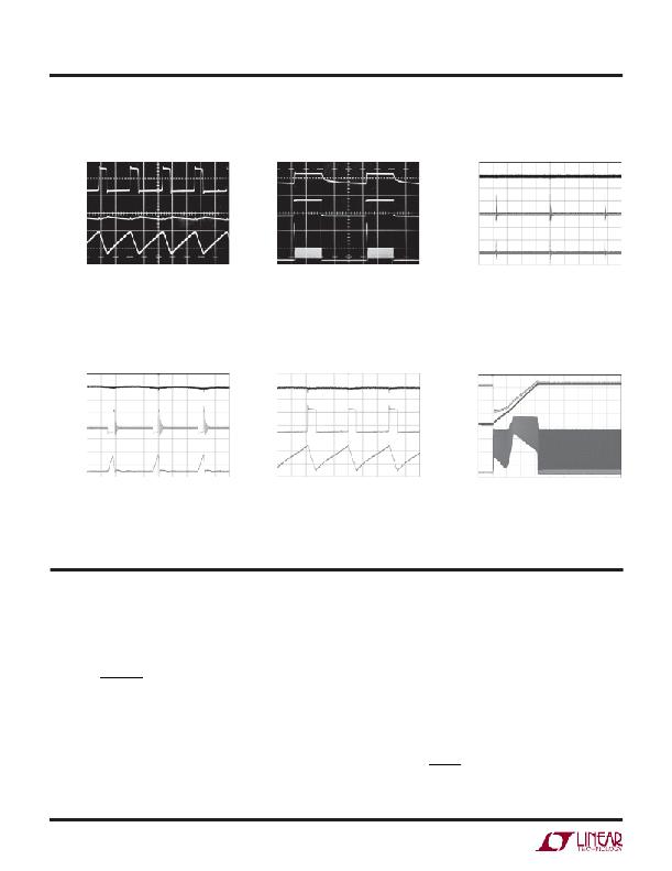
OLED Switching Waveforms
V SW
10V/DIV
V CAP1
50mV/DIV
LED Switching Waveforms
V CAP1
5V/DIV
V CTRL1
5V/DIV
LED Transient Response
V OUT2
10mV/DIV
AC COUPLED
SW2 VOLTAGE
10V/DIV
with No Load
I L
100mA/
DIV
500ns/DIV
V IN = 3.6V
FRONT PAGE APPLICATION
3498 G19
I L
200mA/
DIV
1ms/DIV
V IN = 3.6V
FRONT PAGE APPLICATION
3498 G20
INDUCTOR
CURRENT
50mA/DIV
V IN = 3.6V
V OUT2 = 16V
5μs/DIV
3498 G21
V OUT2
10mV/DIV
AC
COUPLED
SW2
VOLTAGE
10V/DIV
OLED Switching Waveforms
with 4mA Load
V OUT2
10mV/DIV
AC COUPLED
SW2
VOLTAGE
10V/DIV
OLED Switching Waveforms
with 35mA Load
CAP2
VOLTAGE
5V/DIV
V OUT2
VOLTAGE
5V/DIV
OLED Switching Waveforms
During Start-Up
INDUCTOR
CURRENT
200mA/DIV
V IN = 3.6V
V OUT2 = 16V
2μs/DIV
3498 G22
INDUCTOR
CURRENT
200mA/DIV
V IN = 3.6V
V OUT2 = 16V
500ns/DIV
3498 G23
INDUCTOR
CURRENT
100mA/DIV
V IN = 3.6V
V OUT2 = 16V
500μs/DIV
3498 G24
PIN FUNCTIONS
LED1 (Pin 1): Connection Point Between the Anode of the
Highest LED and the Sense Resistor. The LED current can
be programmed by:
CTRL2 (Pin 5): Dimming and Shutdown Pin. Connect
it below 75mV to disable the low noise boost converter.
As the pin voltage is ramped from 0V to 1.5V, the output
I LED 1 =
200mV
R SENSE 1
ramps up to the programmed output voltage.
FB2 (Pin 6): Feedback Pin. Reference voltage is 1.215V.
CTRL1 (Pin 2): Dimming and Shutdown Pin. Connect this
pin below 75mV to disable the white LED driver. As the
There is an internal 182k Ω resistor from FB2 to GND. To
achieve desired output voltage, choose R FB2 according to
the following formula:
pin voltage is ramped from 0V to 1.5V, the LED current
ramps from 0 to (I LED1 = 200mV / R SENSE1 ).
GND1, 2 (Pins 3, 4): Ground. Tie directly to local ground
R FB2 = 182 ?
V OUT2
1.215
1 k
plane. GND1 and GND2 are connected internally.
3498fa
6
发布紧急采购,3分钟左右您将得到回复。
相关PDF资料
LT3517HUF#PBF
IC LED DRIVER AUTOMOTIVE 16-QFN
LT3519EMS-2#PBF
IC LED DRVR HP CONST CURR 16MSOP
LT3590ESC8#TRMPBF
IC LED DRVR WHITE BCKLGT SC-70-8
LT3591EDDB#TRMPBF
IC LED DRIVER WHITE BCKLGT 8-DFN
LT3593ES6#TRMPBF
IC LED DRIVR WHITE BCKLGT TSOT-6
LT3595AEUHH#TRPBF
IC LED DRIVR WHITE BCKLGT 56-QFN
LT3595EUHH#TRPBF
IC LED DRIVR WHITE BCKLGT 56-QFN
LT3596EUHG#PBF
IC LED DVR 300MA ADJ 52-VQFN
相关代理商/技术参数
LT34-SC
制造商:THOMAS & BETTS 功能描述:
LT3500
制造商:World Products 功能描述:
LT3500EDD#PBF
功能描述:IC REG DL BUCK/LINEAR 12-DFN RoHS:是 类别:集成电路 (IC) >> PMIC - 稳压器 - 线性 + 切换式 系列:- 标准包装:2,500 系列:- 拓扑:降压(降压)同步(3),线性(LDO)(2) 功能:任何功能 输出数:5 频率 - 开关:300kHz 电压/电流 - 输出 1:控制器 电压/电流 - 输出 2:控制器 电压/电流 - 输出 3:控制器 带 LED 驱动器:无 带监控器:无 带序列发生器:是 电源电压:5.6 V ~ 24 V 工作温度:-40°C ~ 85°C 安装类型:* 封装/外壳:* 供应商设备封装:* 包装:*
LT3500EDD#TRPBF
功能描述:IC REG DL BUCK/LINEAR 12-DFN RoHS:是 类别:集成电路 (IC) >> PMIC - 稳压器 - 线性 + 切换式 系列:- 标准包装:2,500 系列:- 拓扑:降压(降压)同步(3),线性(LDO)(2) 功能:任何功能 输出数:5 频率 - 开关:300kHz 电压/电流 - 输出 1:控制器 电压/电流 - 输出 2:控制器 电压/电流 - 输出 3:控制器 带 LED 驱动器:无 带监控器:无 带序列发生器:是 电源电压:5.6 V ~ 24 V 工作温度:-40°C ~ 85°C 安装类型:* 封装/外壳:* 供应商设备封装:* 包装:*
LT3500EDD-PBF
制造商:LINER 制造商全称:Linear Technology 功能描述:Monolithic 2A Step-Down Regulator Plus Linear Regulator/Controller
LT3500EDD-TRPBF
制造商:LINER 制造商全称:Linear Technology 功能描述:Monolithic 2A Step-Down Regulator Plus Linear Regulator/Controller
LT3500EMSE#PBF
功能描述:IC REG DL BUCK/LINEAR 16-MSOP RoHS:是 类别:集成电路 (IC) >> PMIC - 稳压器 - 线性 + 切换式 系列:- 标准包装:2,500 系列:- 拓扑:降压(降压)同步(3),线性(LDO)(2) 功能:任何功能 输出数:5 频率 - 开关:300kHz 电压/电流 - 输出 1:控制器 电压/电流 - 输出 2:控制器 电压/电流 - 输出 3:控制器 带 LED 驱动器:无 带监控器:无 带序列发生器:是 电源电压:5.6 V ~ 24 V 工作温度:-40°C ~ 85°C 安装类型:* 封装/外壳:* 供应商设备封装:* 包装:*
LT3500EMSE#TRPBF
功能描述:IC REG DL BUCK/LINEAR 16-MSOP RoHS:是 类别:集成电路 (IC) >> PMIC - 稳压器 - 线性 + 切换式 系列:- 标准包装:2,500 系列:- 拓扑:降压(降压)同步(3),线性(LDO)(2) 功能:任何功能 输出数:5 频率 - 开关:300kHz 电压/电流 - 输出 1:控制器 电压/电流 - 输出 2:控制器 电压/电流 - 输出 3:控制器 带 LED 驱动器:无 带监控器:无 带序列发生器:是 电源电压:5.6 V ~ 24 V 工作温度:-40°C ~ 85°C 安装类型:* 封装/外壳:* 供应商设备封装:* 包装:*
